- 您现在的位置:买卖IC网 > Sheet目录1223 > KIT34674EPEVBE (Freescale Semiconductor)KIT EVAL BOARD 10CH LED BACKLGHT
�� �
�
�TYPICAL� APPLICATIONS�
�INTRODUCTION�
�When� the� battery� voltage� rises� above� the� trickle� charge�
�threshold,� the� charger� enters� the� CC-mode.� The� MC34674�
�tries� to� raise� the� charge� current� to� the� internally� set� reference,�
�such� as� 1.05� A,� by� enhancing� the� power� MOSFET.� However,�
�since� the� current� provided� by� the� AC/DC� regulator� is� limited�
�and� can� never� reach� the� set� reference,� the� charger� will� keep�
�enhancing� the� MOSFET� until� it� is� fully� enhanced� and� is� fully�
�VIN�
�turned� on.� In� this� mode,� the� internal� power� MOSFET� behaves�
�as� a� switch� instead� of� a� linearly� regulating� device.� The�
�voltage� difference� between� the� input� and� the� output� is�
�determined� by� the� on� resistance,� R� DS(ON)� ,� of� the� power�
�MOSFET� and� the� limited� output� current� of� the� ad/dc�
�regulator.�
�R� 1�
�GRN�
�RED�
�V� IN� –� V� OUT� =� I� LIM� ×� R� DS� (� ON� )�
�The� power� dissipation,� P� D� ,� in� the� MOSFET� can� be� calculated�
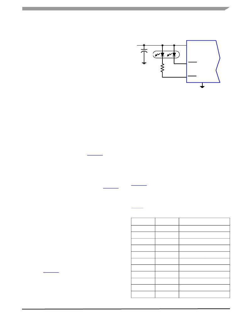
�Figure� 27.� LED� Color� Balancing� Scheme.�
�as,�
�P� D� =� I� LIM� � I� LIM� � R� DS� (� ON� )�
�INPUT� CAPACITOR�
�The� input� capacitor� is� used� to� reduce� the� input� voltage�
�The� charge� current� in� CC-mode� is� not� determined� by� the�
�MC34674,� instead,� it� is� determined� by� the� AC/DC� regulator�
�current� limit,� I� LIM� ,� which� is� a� value� lower� than� the� charger�
�internally� set� current� reference.� The� internally� set� current�
�reference� is� used� as� a� secondary� protection� threshold,� in�
�case� if� an� AC/DC� regulator� with� a� wrong� current� limit� is�
�connected� to� the� input.�
�The� key� advantage� of� using� the� MC34674� with� a� current-�
�limited� AC/DC� regulator� is� the� significant� reduction� of� the�
�power� dissipation� during� the� CC-mode.� Figure 26� illustrates�
�the� small� voltage� difference� between� the� input� and� the� output�
�of� the� charger,� which� is� directly� proportional� to� the� power�
�dissipation.�
�When� entering� the� CC-mode,� the� charger� output� I/V�
�trajectory� jumps� from� point� b� to� c� and� then� moves� from� c� to� d�
�as� the� battery� voltage� rises� to� 4.2� V.� The� AC/DC� regulator�
��When� the� battery� voltage� reaches� the� target� 4.2V,� the�
�charger� enters� the� CV-mode.� The� charge� current� starts� to�
�decline� and� the� AC/DC� regulator� output� enters� its� constant-�
�voltage� mode.� The� charger� then� operates� as� a� regular� linear�
�charger� again� until� the� charging� completes.� The� battery� I/V�
�trajectory� moves� from� d� to� the� EOC� moment� (point� e� )� while�
�transient� that� may� cause� instability.� A� 1.0� μ� F,� X5R,� 16� V�
�rated� ceramic� capacitor� is� recommended� for� most�
�applications.�
�OUTPUT� CAPACITOR�
�For� stable� operation,� an� X5R� ceramic� capacitor� with� a�
�minimum� 1.0� μ� F� nominal� value� is� recommended� at� the�
�output.� The� output� capacitance� should� not� be� larger� than�
�240� μ� F� to� allow� the� 585� μ� A� current� to� discharge� the� capacitor�
�voltage� to� the� recharge� threshold� within� 82� ms.�
�NTC� INTERFACE� DESIGN�
�The� NTC� interface� is� designed� to� be� able� to� work� with� most�
�types� of� NTC� thermistors.� This� section� describes� in� details�
�how� to� select� the� two� resistors� R� U� and� R� S� shown� in�
��temperature� thresholds� are� discussed.� The�
�NCP15W104F03RC� from� Murata� is� used� as� an� example� for�
�the� calculations� in� this� section.� The� partial� temperature�
�characteristics� of� the� NCP15W104F03RC� are� given� in�
��Table 7. NTC Thermistor Temperature Characteristics.�
�the� AC/DC� regulator� output� trajectory� jumps� from� C� to� D� and�
�then� moves� to� E� at� the� EOC� moment.�
�BALANCING� YELLOW� COLOR� IN� LED�
�The� red� and� the� green� colors� in� the� LED� are� driven� by� two�
�matched� 6.0� mA� current� sources.� Such� design� ensured� a�
�consistent� brightness� of� the� LED� over� a� large� range� of� the�
�input� voltage.� When� both� colors� are� turned� on,� the� resulting�
�color� should� be� yellow.� One� can� adjust� the� resulting� color� by�
�Temp� (°C)�
�-2�
�-1�
�0�
�2�
�3�
�R-low� (k� Ω� )�
�389.2453�
�368.4960�
�348.9722�
�313.2543�
�296.9408�
�R-center� (k� Ω� )�
�398.6521�
�377.1927�
�357.0117�
�320.1216�
�303.2866�
�R-high� (k� Ω� )�
�408.2455�
�386.0560�
�365.1999�
�327.1067�
�309.7370�
�adjusting� the� brightness� of� the� individual� color.� A� resistor� can�
�...�
�be� added� to� reduce� the� brightness� of� one� color,� such� as� the�
��46�
�47�
�50�
�53�
�54�
�38.4596�
�36.8626�
�32.5022�
�28.7183�
�27.5694�
�39.2132�
�37.6010�
�33.1946�
�29.3660�
�28.2026�
�39.9778�
�28.3503�
�33.8983�
�30.0253�
�28.8474�
�34674�
�Analog� Integrated� Circuit� Device� Data�
�Freescale� Semiconductor�
�21�
�发布紧急采购,3分钟左右您将得到回复。
相关PDF资料
KIT34675EPEVBE
KIT EVALUATION FOR MC34675
KIT35XS3500EVBE
KIT EVAL QUAD HIGH SIDE SWITCH
KITUSBSPIEVME
KIT EVAL USB-SPI W/MC68HC908JW32
KP3040
KEYPAD USB W/2 USB PORTS
KS8737-EVAL
BOARD EVAL EXPERIMENT FOR KS8737
KSZ8695PX-EVAL
KIT EVAL KSZ8695PX EXPERIMENT
KSZ9692PB-EVAL
BOARD EVALUATION FOR KSZ9692PB
L17-RR-D1-F-01-100
CONN SOCKET 20-24AWG CRIMP GOLD
相关代理商/技术参数
KIT34675EPEVBE
功能描述:电源管理IC开发工具 28V-INPUT-VOLT SNGL RoHS:否 制造商:Maxim Integrated 产品:Evaluation Kits 类型:Battery Management 工具用于评估:MAX17710GB 输入电压: 输出电压:1.8 V
KIT34676EPEVBE
功能描述:电源管理IC开发工具 DUAL 28V-INPUTVOLT C RoHS:否 制造商:Maxim Integrated 产品:Evaluation Kits 类型:Battery Management 工具用于评估:MAX17710GB 输入电压: 输出电压:1.8 V
KIT34676EPEVBE
制造商:Freescale Semiconductor 功能描述:Dual 28V input voltage single cell Li-Io
KIT3468MMA7455L
功能描述:加速传感器开发工具 3-AXIS 2G ,4G, 8G Dig Out, Dev Kit RoHS:否 制造商:Murata 工具用于评估:SCA3100-D04 加速:2 g 传感轴:Triple Axis 接口类型:SPI 工作电压:3.3 V
KIT3468MMA7455L
制造商:Freescale Semiconductor 功能描述:Output Accelerometer Evaluation Board
KIT3468MMA7456L
功能描述:加速传感器开发工具 XYZ-AXIS DIGITAL 2G4G RoHS:否 制造商:Murata 工具用于评估:SCA3100-D04 加速:2 g 传感轴:Triple Axis 接口类型:SPI 工作电压:3.3 V
KIT34700EPEVBE
功能描述:电源管理IC开发工具 4 Output Integrated Pwr Supply Eval Kit RoHS:否 制造商:Maxim Integrated 产品:Evaluation Kits 类型:Battery Management 工具用于评估:MAX17710GB 输入电压: 输出电压:1.8 V
KIT34703PNBEVBE
功能描述:电源管理IC开发工具 10 A SWTCH-MODE PWR S RoHS:否 制造商:Maxim Integrated 产品:Evaluation Kits 类型:Battery Management 工具用于评估:MAX17710GB 输入电压: 输出电压:1.8 V